
SEMI-CONDUCTOR
Semiconductor is a huge field, and one of its biggest areas is IC designing. IC or Integrated Circuits contains several transistors fabricated on a single chip. A VLSI (Very Large Scale Integration) system integrates millions (30000 – 1000000) of “electronic components” in a small area (few mm²-> few cm²).To design anything we need like a Microprocessor, Microcontroller, Memory, Printer, Mobile, Digital security lock in a word everything of our day-to-day use needs a chip. This chip is the ultimate design of a VLSI design flow. Which actually goes through as following way: We need idea-> Specification-> design architecture-> Functional verification-> Logic design-> Logic verification-> Circuit Design-> Circuit Verification-> Physical design-> Layout verification-> Fabrication & testing-> IC chip.
To perform this whole flow we need EDA (electric design automation) tools. From lots of EDA tools, we focused on Cadence EDA tools. It covers the whole design of an IC chip.
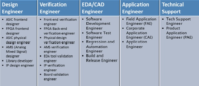
Furthermore, the field of opportunities of VLSI is huge, we can take a glance as mentioned here:
Here we mention that we are the pioneer Provider of Cadence tools in Bangladesh. Cadence EDA tools have lots of features. Founded in 1988, its revenues will be approximately $1.46 billion by 2013. Cadence EDA tools span the entire product development process.